gdsfactory includes a generic PDK gdsfactory.generic_tech that you can use as an inspiration to create your own. It is based on the book “Silicon Photonics Design: From Devices to Systems Lukas Chrostowski, Michael Hochberg”.
The PDK technology also includes a generic component library that you can use to create your own components.
LayerMap
A layer map maps layer names to a integer numbers pair (GDSlayer, GDSpurpose)
Each foundry uses different GDS layer numbers for different process steps.
| GDS (layer, purpose) | layer_name | Description |
|---|---|---|
| 1 , 0 | WG | 220 nm Silicon core |
| 2 , 0 | SLAB150 | 150nm Silicon slab (70nm shallow Etch for grating couplers) |
| 3 , 0 | SLAB90 | 90nm Silicon slab (for modulators) |
| 4, 0 | DEEPTRENCH | Deep trench |
| 47, 0 | MH | heater |
| 41, 0 | M1 | metal 1 |
| 45, 0 | M2 | metal 2 |
| 40, 0 | VIAC | VIAC to contact Ge, NPP or PPP |
| 44, 0 | VIA1 | VIA1 |
| 46, 0 | PADOPEN | Bond pad opening |
| 51, 0 | UNDERCUT | Undercut |
| 66, 0 | TEXT | Text markup |
| 64, 0 | FLOORPLAN | Mask floorplan |
from pydantic import BaseModel

import gdsfactory as gf
from gdsfactory.generic_tech import LAYER, LAYER_STACK
from gdsfactory.generic_tech.get_klayout_pyxs import get_klayout_pyxs
from gdsfactory.technology import LayerLevel, LayerStack, LayerViews, LayerMap
from gdsfactory.generic_tech import get_generic_pdk
from IPython.display import Code

from gdsfactory.config import PATH
Layer = tuple[int, int]
gf.config.rich_output()
PDK = get_generic_pdk()
PDK.activate()
class GenericLayerMap(LayerMap):
"""Generic layermap based on book.
Lukas Chrostowski, Michael Hochberg, "Silicon Photonics Design",
Cambridge University Press 2015, page 353
You will need to create a new LayerMap with your specific foundry layers.
"""
WAFER: Layer = (99999, 0)
WG: Layer = (1, 0)
WGCLAD: Layer = (111, 0)
SLAB150: Layer = (2, 0)
SLAB90: Layer = (3, 0)
DEEPTRENCH: Layer = (4, 0)
GE: Layer = (5, 0)
UNDERCUT: Layer = (6, 0)
WGN: Layer = (34, 0)
WGN_CLAD: Layer = (36, 0)
N: Layer = (20, 0)
NP: Layer = (22, 0)
NPP: Layer = (24, 0)
P: Layer = (21, 0)
PP: Layer = (23, 0)
PPP: Layer = (25, 0)
GEN: Layer = (26, 0)
GEP: Layer = (27, 0)
HEATER: Layer = (47, 0)
M1: Layer = (41, 0)
M2: Layer = (45, 0)
M3: Layer = (49, 0)
VIAC: Layer = (40, 0)
VIA1: Layer = (44, 0)
VIA2: Layer = (43, 0)
PADOPEN: Layer = (46, 0)
DICING: Layer = (100, 0)
NO_TILE_SI: Layer = (71, 0)
PADDING: Layer = (67, 0)
DEVREC: Layer = (68, 0)
FLOORPLAN: Layer = (64, 0)
TEXT: Layer = (66, 0)
PORT: Layer = (1, 10)
PORTE: Layer = (1, 11)
PORTH: Layer = (70, 0)
SHOW_PORTS: Layer = (1, 12)
LABEL: Layer = (201, 0)
LABEL_SETTINGS: Layer = (202, 0)
DRC_MARKER: Layer = (205, 0)
LABEL_INSTANCE: Layer = (206, 0)
SOURCE: Layer = (110, 0)
MONITOR: Layer = (101, 0)
LAYER = GenericLayerMap()
LAYERlayer_wg = (1, 0)
print(layer_wg)(1, 0)
Extract layers
You can also extract layers using the extract function. This function returns a new flattened Component that contains the extracted layers.
A flat Component does not have references, and all the polygons are absorbed into the top cell.
from gdsfactory.generic_tech import get_generic_pdk

PDK = get_generic_pdk()
PDK.activate()

LAYER_VIEWS = PDK.layer_views
c = LAYER_VIEWS.preview_layerset()
c.plot()extract = c.extract(layers=((41, 0), (40, 0)))
extract.plot()Remove layers
You can remove layers using the remove_layers() function.
removed = extract.remove_layers(layers=((40, 0),))
removed.plot()Remap layers
You can remap (change the polygons from one layer to another layer) using the remap_layer, which will return a new Component
c = gf.components.straight(layer=(2, 0))
c.plot()remap = c.remap_layers(layermap={(2, 0): (34, 0)})
remap.plot()LayerViews
Klayout shows each GDS layer with a color, style and transparency
You can define your layerViews in a klayout Layer Properties file layers.lyp or in YAML format
We recommend using YAML and then generate the lyp in klayout, as YAML is easier to modify than XML.
Code(filename=PATH.klayout_yaml)Once you modify the YAML file you can easily write it to klayout layer properties lyp or the other way around.
YAML <---> LYPThe functions LayerView.to_lyp(filepath) and LayerView.to_yaml(filepath) allow you to convert from each other.
LYP is based on XML so it’s much easier to make changes and maintain the equivalent YAML file.
YAML -> LYP
You can easily convert from YAML into Klayout Layer Properties.
LAYER_VIEWS = LayerViews(filepath=PATH.klayout_lyp)
LAYER_VIEWS.to_lyp("extra/klayout_layers.lyp")LYP -> YAML
Sometimes you start from an LYP XML file. We recommend converting to YAML and using the YAML as the layer views source of truth.
Layers in YAML are easier to read and modify than doing it in klayout XML format.
LAYER_VIEWS = LayerViews(filepath=PATH.klayout_lyp)
LAYER_VIEWS.to_yaml("extra/layers.yaml")
2023-12-09 17:29:49.207 | INFO | gdsfactory.technology.layer_views:__init__:785 - Importing LayerViews from KLayout layer properties file: '/home/runner/work/gdsfactory/gdsfactory/gdsfactory/generic_tech/klayout/tech/layers.lyp'.
Preview layerset
You can preview all the layers defined in your LayerViews
c = LAYER_VIEWS.preview_layerset()
c.plot()By default the generic PDK has some layers that are not visible and therefore are not shown.
c_wg_clad = c.extract(layers=(1, 0))
c_wg_clad.plot()LAYER_VIEWS.layer_views["WGCLAD"]LAYER_VIEWS.layer_views["WGCLAD"].visibleYou can make it visible
LAYER_VIEWS.layer_views["WGCLAD"].visible = TrueLAYER_VIEWS.layer_views["WGCLAD"].visiblec_wg_clad = c.extract(layers=(111, 0))
c_wg_clad.plot()LayerStack
Each layer also includes the information of thickness and position of each layer after fabrication.
This LayerStack can be used for creating a 3D model with Component.to_3d or running Simulations.
A GDS has different layers to describe the different fabrication process steps. And each grown layer needs thickness information and z-position in the stack.
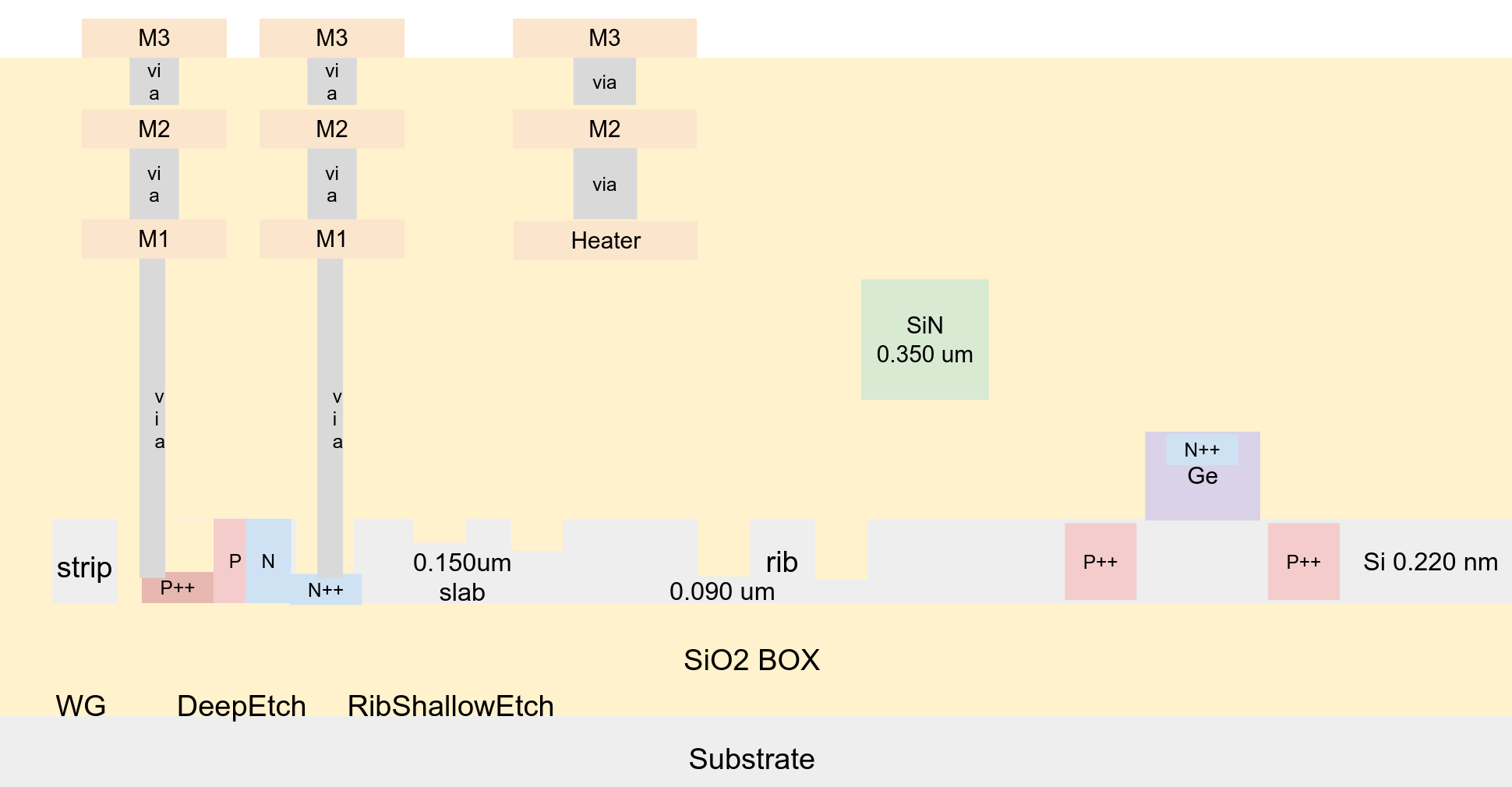
Lets define the layer stack for the generic layers in the generic_technology.
from gdsfactory.generic_tech.layer_map import LAYER
from gdsfactory.technology import LayerLevel, LayerStack

nm = 1e-3


def get_layer_stack(
    thickness_wg: float = 220 * nm,
    thickness_slab_deep_etch: float = 90 * nm,
    thickness_slab_shallow_etch: float = 150 * nm,
    sidewall_angle_wg: float = 10,
    thickness_clad: float = 3.0,
    thickness_nitride: float = 350 * nm,
    thickness_ge: float = 500 * nm,
    gap_silicon_to_nitride: float = 100 * nm,
    zmin_heater: float = 1.1,
    zmin_metal1: float = 1.1,
    thickness_metal1: float = 700 * nm,
    zmin_metal2: float = 2.3,
    thickness_metal2: float = 700 * nm,
    zmin_metal3: float = 3.2,
    thickness_metal3: float = 2000 * nm,
    substrate_thickness: float = 10.0,
    box_thickness: float = 3.0,
    undercut_thickness: float = 5.0,
) -> LayerStack:
    """Returns generic LayerStack.

    based on paper https://www.degruyter.com/document/doi/10.1515/nanoph-2013-0034/html

    Args:
        thickness_wg: waveguide thickness in um.
        thickness_slab_deep_etch: for deep etched slab.
        thickness_shallow_etch: thickness for the etch.
        sidewall_angle_wg: waveguide side angle.
        thickness_clad: cladding thickness in um.
        thickness_nitride: nitride thickness in um.
        thickness_ge: germanium thickness.
        gap_silicon_to_nitride: distance from silicon to nitride in um.
        zmin_heater: TiN heater.
        zmin_metal1: metal1.
        thickness_metal1: metal1 thickness.
        zmin_metal2: metal2.
        thickness_metal2: metal2 thickness.
        zmin_metal3: metal3.
        thickness_metal3: metal3 thickness.
        substrate_thickness: substrate thickness in um.
        box_thickness: bottom oxide thickness in um.
        undercut_thickness: thickness of the silicon undercut.
    """

    thickness_deep_etch = thickness_wg - thickness_slab_deep_etch
    thickness_shallow_etch = thickness_wg - thickness_slab_shallow_etch

    return LayerStack(
        layers=dict(
            substrate=LayerLevel(
                layer=LAYER.WAFER,
                thickness=substrate_thickness,
                zmin=-substrate_thickness - box_thickness,
                material="si",
                mesh_order=101,
                background_doping={"concentration": "1E14", "ion": "Boron"},
                orientation="100",
            ),
            box=LayerLevel(
                layer=LAYER.WAFER,
                thickness=box_thickness,
                zmin=-box_thickness,
                material="sio2",
                mesh_order=9,
            ),
            core=LayerLevel(
                layer=LAYER.WG,
                thickness=thickness_wg,
                zmin=0.0,
                material="si",
                mesh_order=2,
                sidewall_angle=sidewall_angle_wg,
                width_to_z=0.5,
                background_doping_concentration=1e14,
                background_doping_ion="Boron",
                orientation="100",
                info={"active": True},
            ),
            shallow_etch=LayerLevel(
                layer=LAYER.SHALLOW_ETCH,
                thickness=thickness_shallow_etch,
                zmin=0.0,
                material="si",
                mesh_order=1,
                layer_type="etch",
                into=["core"],
                derived_layer=LAYER.SLAB150,
            ),
            deep_etch=LayerLevel(
                layer=LAYER.DEEP_ETCH,
                thickness=thickness_deep_etch,
                zmin=0.0,
                material="si",
                mesh_order=1,
                layer_type="etch",
                into=["core"],
                derived_layer=LAYER.SLAB90,
            ),
            clad=LayerLevel(
                # layer=LAYER.WGCLAD,
                layer=LAYER.WAFER,
                zmin=0.0,
                material="sio2",
                thickness=thickness_clad,
                mesh_order=10,
            ),
            slab150=LayerLevel(
                layer=LAYER.SLAB150,
                thickness=150e-3,
                zmin=0,
                material="si",
                mesh_order=3,
            ),
            slab90=LayerLevel(
                layer=LAYER.SLAB90,
                thickness=thickness_slab_deep_etch,
                zmin=0.0,
                material="si",
                mesh_order=2,
            ),
            nitride=LayerLevel(
                layer=LAYER.WGN,
                thickness=thickness_nitride,
                zmin=thickness_wg + gap_silicon_to_nitride,
                material="sin",
                mesh_order=2,
            ),
            ge=LayerLevel(
                layer=LAYER.GE,
                thickness=thickness_ge,
                zmin=thickness_wg,
                material="ge",
                mesh_order=1,
            ),
            undercut=LayerLevel(
                layer=LAYER.UNDERCUT,
                thickness=-undercut_thickness,
                zmin=-box_thickness,
                material="air",
                z_to_bias=(
                    [0, 0.3, 0.6, 0.8, 0.9, 1],
                    [-0, -0.5, -1, -1.5, -2, -2.5],
                ),
                mesh_order=1,
            ),
            via_contact=LayerLevel(
                layer=LAYER.VIAC,
                thickness=zmin_metal1 - thickness_slab_deep_etch,
                zmin=thickness_slab_deep_etch,
                material="Aluminum",
                mesh_order=1,
                sidewall_angle=-10,
                width_to_z=0,
            ),
            metal1=LayerLevel(
                layer=LAYER.M1,
                thickness=thickness_metal1,
                zmin=zmin_metal1,
                material="Aluminum",
                mesh_order=2,
            ),
            heater=LayerLevel(
                layer=LAYER.HEATER,
                thickness=750e-3,
                zmin=zmin_heater,
                material="TiN",
                mesh_order=2,
            ),
            via1=LayerLevel(
                layer=LAYER.VIA1,
                thickness=zmin_metal2 - (zmin_metal1 + thickness_metal1),
                zmin=zmin_metal1 + thickness_metal1,
                material="Aluminum",
                mesh_order=1,
            ),
            metal2=LayerLevel(
                layer=LAYER.M2,
                thickness=thickness_metal2,
                zmin=zmin_metal2,
                material="Aluminum",
                mesh_order=2,
            ),
            via2=LayerLevel(
                layer=LAYER.VIA2,
                thickness=zmin_metal3 - (zmin_metal2 + thickness_metal2),
                zmin=zmin_metal2 + thickness_metal2,
                material="Aluminum",
                mesh_order=1,
            ),
            metal3=LayerLevel(
                layer=LAYER.M3,
                thickness=thickness_metal3,
                zmin=zmin_metal3,
                material="Aluminum",
                mesh_order=2,
            ),
        )
    )


LAYER_STACK = get_layer_stack()
layer_stack220 = LAYER_STACK
c = gf.components.straight_heater_doped_rib(length=100)
c.plot()scene = c.to_3d(layer_stack=layer_stack220)
scene.show()c = gf.components.straight_heater_metal(length=40)
c.plot()scene = c.to_3d(layer_stack=layer_stack220)
scene.show()c = gf.components.taper_strip_to_ridge_trenches()
c.plot()scene = c.to_3d(layer_stack=layer_stack220)
scene.show()# lets assume we have 900nm silicon instead of 220nm, You will see a much thicker waveguide under the metal heater.
layer_stack900 = get_layer_stack(thickness_wg=900 * nm)
scene = c.to_3d(layer_stack=layer_stack900)
scene.show()import gdsfactory as gf
c = gf.components.grating_coupler_elliptical_trenches()
c.plot()scene = c.to_3d()
scene.show()3D rendering
To render components in 3D you will need to define two things:
- LayerStack: for each layer contains thickness of each material and z position
- LayerViews: for each layer contains view (color, pattern, opacity). You can load it with
gf.technology.LayerView.load_lyp()
heater = gf.components.straight_heater_metal(length=50)
heater.plot()scene = heater.to_3d()
scene.show()Klayout 2.5D view
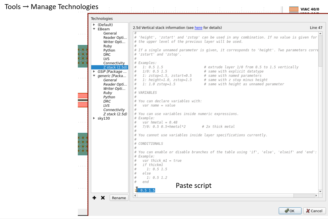
From the LayerStack you can generate the KLayout 2.5D view script.
LAYER_STACK.get_klayout_3d_script()Then you go go Tools → Manage Technologies
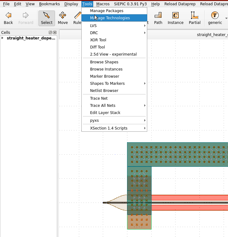
and Paste the 2.5D view script
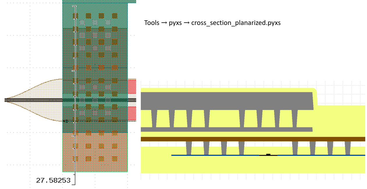
Klayout cross-section
You can also install the KLayout cross-section plugin
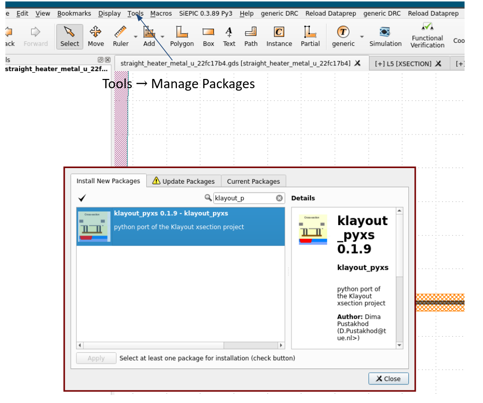
This is not integrated with the LayerStack but you can customize the script in gdsfactory.generic_tech.get_klayout_pyxs for your technology.
nm = 1e-3
if __name__ == "__main__":
    script = get_klayout_pyxs(
        t_box=2.0,
        t_slab=110 * nm,
        t_si=220 * nm,
        t_ge=400 * nm,
        t_nitride=400 * nm,
        h_etch1=0.07,
        h_etch2=0.06,
        h_etch3=0.09,
        t_clad=0.6,
        t_m1=0.5,
        t_m2=0.5,
        t_m3=2.0,
        gap_m1_m2=0.6,
        gap_m2_m3=0.3,
        t_heater=0.1,
        gap_oxide_nitride=0.82,
        t_m1_oxide=0.6,
        t_m2_oxide=2.0,
        t_m3_oxide=0.5,
        layer_wg=(1, 0),
        layer_fc=(2, 0),
        layer_rib=LAYER.SLAB90,
        layer_n=LAYER.N,
        layer_np=LAYER.NP,
        layer_npp=LAYER.NPP,
        layer_p=LAYER.P,
        layer_pp=LAYER.PP,
        layer_ppp=LAYER.PPP,
        layer_PDPP=LAYER.GEP,
        layer_nitride=LAYER.WGN,
        layer_Ge=LAYER.GE,
        layer_GePPp=LAYER.GEP,
        layer_GeNPP=LAYER.GEN,
        layer_viac=LAYER.VIAC,
        layer_viac_slot=LAYER.VIAC,
        layer_m1=LAYER.M1,
        layer_mh=LAYER.HEATER,
        layer_via1=LAYER.VIA1,
        layer_m2=LAYER.M2,
        layer_via2=LAYER.VIA2,
        layer_m3=LAYER.M3,
        layer_open=LAYER.PADOPEN,
    )

    # script_path = pathlib.Path(__file__).parent.absolute() / "xsection_planarized.pyxs"
    # script_path.write_text(script)
    print(script)
t_box=2.0
t_slab=0.11
t_si=0.22
t_ge=0.4
t_nitride=0.4
h_etch1=0.07
h_etch2=0.06
h_etch3=0.09
t_clad=0.6
t_m1=0.5
t_m2=0.5
t_m3=2.0
t_heater=0.1
gap_m1_m2=0.6
gap_m2_m3=0.3
gap_oxide_nitride=0.82
t_m1_oxide=0.6
t_m2_oxide=2.0
t_m3_oxide=0.5

l_wg = layer('1/0')
l_fc = layer('2/0')
l_rib = layer('3/0')

l_n = layer('20/0')
l_np = layer('22/0')
l_npp = layer('24/0')
l_p = layer('21/0')
l_pp = layer('23/0')
l_ppp = layer('25/0')
l_PDPP = layer('27/0')
l_bottom_implant = l_PDPP

l_nitride = layer('34/0')
l_Ge = layer('5/0')
l_GePPp = layer('27/0')
l_GeNPP = layer('26/0')

l_viac = layer('40/0')
l_viac_slot = layer('40/0')
l_m1 = layer('41/0')
l_mh = layer('47/0')
l_via1 = layer('44/0')
l_m2 = layer('45/0')
l_via2 = layer('43/0')
l_m3 = layer('49/0')
l_open = layer('46/0')

l_top_implant = l_GePPp.or_(l_GeNPP)
l_viac = l_viac.or_(l_viac_slot)

# Declare the basic accuracy used to remove artifacts for example: delta(5 * dbu)
delta(dbu)
depth(12.0)
height(12.0)

################ front-end

l_wg_etch1 = l_wg.inverted()  # protects ridge
l_wg_etch2 = (
    l_fc.or_(l_wg)
).inverted()  # protects ridge and grating couplers from the etch down to the slab (forms rib straights)
l_wg_etch3 = (
    l_rib.or_(l_fc).or_(l_wg)
).inverted()  # protects ridge, grating couplers and rib straights from the final etch to form strip straights


################ back-end
substrate = bulk
box = deposit(t_box)
si = deposit(t_si)

################ silicon etch to for the passives
mask(l_wg_etch1).etch(
    h_etch1, 0.0, mode="round", into=[si]
)  # 70nm etch for GC, rib and strip
mask(l_wg_etch2).etch(
    h_etch2, 0.0, mode="round", into=[si]
)  # 60nm etch after 70nm = 130nm etch (90nm slab)
mask(l_wg_etch3).etch(
    h_etch3, 0.0, mode="round", into=[si]
)  # etches the remaining 90nm slab for strip straights

output("300/0", box)
output("301/0", si)

############### doping
mask(l_bottom_implant).etch(t_si, 0.0, mode="round", into=[si])
bottom_implant = mask(l_bottom_implant).grow(t_si, 0.0, mode="round")

mask(l_n).etch(t_slab, 0.0, mode="round", into=[si])
n = mask(l_n).grow(t_slab, 0.0, mode="round")

mask(l_p).etch(t_slab, 0.0, mode="round", into=[si])
p = mask(l_p).grow(t_slab, 0.0, mode="round")

mask(l_np).etch(t_slab, 0.0, mode="round", into=[n, p, si, bottom_implant])
np = mask(l_np).grow(t_slab, 0.0, mode="round")

mask(l_pp).etch(t_slab, 0.0, mode="round", into=[n, p, si, bottom_implant])
pp = mask(l_pp).grow(t_slab, 0.0, mode="round")

mask(l_npp).etch(t_slab, 0.0, mode="round", into=[n, p, np, pp, si, bottom_implant])
npp = mask(l_npp).grow(t_slab, 0.0, mode="round")

mask(l_ppp).etch(t_slab, 0.0, mode="round", into=[n, p, np, pp, si, bottom_implant])
ppp = mask(l_ppp).grow(t_slab, 0.0, mode="round")

output("327/0", bottom_implant)
output("330/0", p)
output("320/0", n)
output("321/0", npp)
output("331/0", ppp)

################ Ge
Ge = mask(l_Ge).grow(t_ge, 0, bias=0.0, taper=10)
output("315/0", Ge)

################ Nitride
ox_nitride = deposit(2 * gap_oxide_nitride, 2 * gap_oxide_nitride)
planarize(less=gap_oxide_nitride, into=[ox_nitride])
output("302/0", ox_nitride)

nitride = mask(l_nitride).grow(t_nitride, 0, bias=0.0, taper=10)
output("305/0", nitride)

################# back-end
################# VIAC, M1 and MH
ox_nitride_clad = deposit(t_clad + t_ge + t_nitride, t_clad + t_ge + t_nitride, mode="round")

planarize(less=t_ge + t_nitride, into=[ox_nitride_clad])
mask(l_viac).etch(
    t_clad + t_ge + t_nitride + gap_oxide_nitride, taper=4, into=[ox_nitride_clad, ox_nitride]
)

viac = deposit(2 * t_clad, 2 * t_clad)
planarize(less=2 * t_clad, into=[viac])

mh = deposit(t_heater, t_heater)
mask(l_mh.inverted()).etch(t_heater + t_heater, into=[mh])
m1 = deposit(t_m1, t_m1)
mask(l_m1.inverted()).etch(t_m1 + t_m1, into=[m1])
output("306/0", mh)
output("399/0", m1)

output("304/0", ox_nitride_clad)
output("303/0", viac)

################# VIA1 and M2
ox_m1 = deposit(2 * t_m1_oxide, 2 * t_m1_oxide, mode="round")
planarize(less=t_m1_oxide, into=[ox_m1])

mask(l_via1).etch(t_m1_oxide + gap_m1_m2, taper=4, into=[ox_m1])
via1 = deposit(t_m2, t_m2)

mask(l_m2.inverted()).etch(t_m2, taper=4, into=[via1])
output("308/0", via1)

ox_m2 = deposit(2 * t_m2_oxide, 2 * t_m2_oxide, mode="round")
planarize(less=t_m2_oxide, into=[ox_m2])
output("309/0", ox_m2)
output("307/0", ox_m1)

################# VIA2 and M3
mask(l_via2).etch(t_m2_oxide + gap_m2_m3, taper=4, into=[ox_m2, ox_m2])
via2 = deposit(t_m3, t_m3)
mask(l_m3.inverted()).etch(t_m3, taper=4, into=[via2])
output("310/0", via2)

################# passivation and ML Open
ox_m3 = deposit(t_m3_oxide, t_m3_oxide, mode="round")
mask(l_open).etch(t_m3_oxide + t_m3_oxide, into=[ox_m3], taper=5)
output("311/0", ox_m3)
Process
The LayerStack uses the GDS layers to generate a representation of the chip after fabrication.
The KLayout cross-section module uses the GDS layers to return a geometric approximation of the processed wafer.
Sometimes, however, physical process modeling is desired.
For these purposes, Processes acting on an initial substrate “wafer stack” can be defined. The waferstack is a LayerStack representing the initial state of the wafer. The processes take in some combination of GDS layers (which may differ from their use in the resulting LayerStack), some processing parameters, and are then run in a sequence.
For instance, the early step of the front-end-of-line of the generic process could be approximated as done in gdsfactory.technology.layer_stack (the process classes are described in gdsfactory.technology.processes):
import gdsfactory.technology.processes as gp


def get_process():
    """Returns generic process to generate LayerStack.

    Represents processing steps that will result in the GenericLayerStack, starting from the waferstack LayerStack.

    based on paper https://www.degruyter.com/document/doi/10.1515/nanoph-2013-0034/html
    """

    return (
        gp.Etch(
            name="strip_etch",
            layer=(1, 0),
            positive_tone=False,
            depth=0.22 + 0.01,  # slight overetch for numerics
            material="core",
            resist_thickness=1.0,
        ),
        gp.Etch(
            name="slab_etch",
            layer=LAYER.SLAB90,
            layers_diff=[(1, 0)],
            depth=0.22 - 0.09,
            material="core",
            resist_thickness=1.0,
        ),
        # See gplugins.process.implant tables for ballpark numbers
        # Adjust to your process
        gp.ImplantPhysical(
            name="deep_n_implant",
            layer=LAYER.N,
            energy=100,
            ion="P",
            dose=1e12,
            resist_thickness=1.0,
        ),
        gp.ImplantPhysical(
            name="shallow_n_implant",
            layer=LAYER.N,
            energy=50,
            ion="P",
            dose=1e12,
            resist_thickness=1.0,
        ),
        gp.ImplantPhysical(
            name="deep_p_implant",
            layer=LAYER.P,
            energy=50,
            ion="B",
            dose=1e12,
            resist_thickness=1.0,
        ),
        gp.ImplantPhysical(
            name="shallow_p_implant",
            layer=LAYER.P,
            energy=15,
            ion="B",
            dose=1e12,
            resist_thickness=1.0,
        ),
        # "Temperatures of ~1000C for not more than a few seconds"
        # Adjust to your process
        # https://en.wikipedia.org/wiki/Rapid_thermal_processing
        gp.Anneal(
            name="dopant_activation",
            time=1,
            temperature=1000,
        ),
    )


process = get_process()
These process dataclasses can then be used in physical simulator plugins.